EC3552 – VLSI And Chip Design Syllabus Regulation 2021 Anna University
Code EC3552 deals with the subject from the Anna University Regulation 2021, related to affiliated institutions, syllabus of B.E Electronics and Telecommunication Engineering. In this article, we discuss the VLSI And Chip Design Syllabus.
We intend to provide the syllabus of EC3552 – VLSI And Chip Design, we include the textbooks and references from the faculty of experts. You can get the required information unit-wise. The following links will help you to get proper information. I hope you can find the details in the article given below.
If you want to know more about the syllabus of B.E Computer Science and Engineering (Cyber security) Syllabus connected to an affiliated institution’s four-year undergraduate degree program. We provide you with a detailed Year-wise, semester-wise, and Subject-wise syllabus in the following link B.E Electronics and Telecommunication Engineering Syllabus Anna University, Regulation 2021.
Aim of Objectives:
- Understand the fundamentals of IC technology components and their characteristics.
- Understand combinational logic circuits and design principles.
- Understand sequential logic circuits and clocking strategies.
- Understand ASIC Design functioning and design.
- Understand Memory Architecture and building blocks.
EC3552 – VLSI And Chip Design Syllabus
Unit – I: MOS Transistor Principles
MOS logic families (NMOS and CMOS), Ideal and Non Ideal IV Characteristics, CMOS devices. MOS(FET) Transistor Characteristic under Static and Dynamic Conditions, Technology Scaling, Power Consumption.
Unit – II: Combinational Logic Circuits
Propagation Delays, stick diagram, Layout diagrams, Examples of combinational logic design, Elmore’s constant, Static Logic Gates, Dynamic Logic Gates, Pass Transistor Logic, Power Dissipation, Low Power Design principles.
Unit – III: Sequential Logic Circuits And Clocking Strategies
Static Latches and Registers, Dynamic Latches and Registers, Pipelines, Nonbistable Sequential Circuits.Timing classification of Digital Systems, Synchronous Design, Self-Timed Circuit Design.
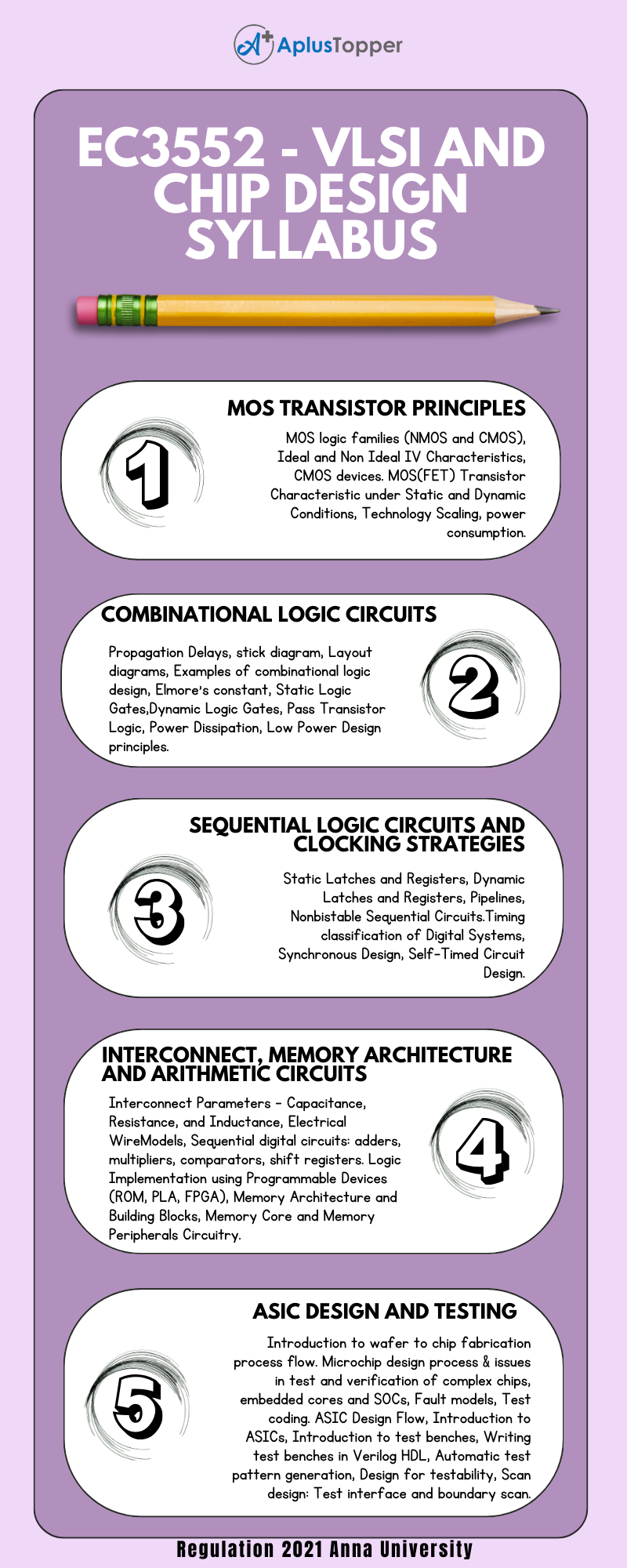
Unit – IV: Interconnect, Memory Architecture And Arithmetic Circuits
Interconnect Parameters – Capacitance, Resistance, and Inductance, Electrical WireModels, Sequential digital circuits: adders, multipliers, comparators, shift registers. Logic Implementation using Programmable Devices (ROM, PLA, FPGA), Memory Architecture and Building Blocks, Memory Core and Memory Peripherals Circuitry.
Unit – V: Asic Design And Testing
Introduction to wafer-to-chip fabrication process flow. Microchip design process & issues in test and verification of complex chips, embedded cores, and SOCs, Fault models, Test coding. ASIC Design Flow, Introduction to ASICs, Introduction to test benches, Writing test benches in Verilog HDL, Automatic test pattern generation, Design for testability, Scan design: Test interface and boundary scan.
Text Books:
- Jan D Rabaey, Anantha Chandrakasan, “Digital Integrated Circuits: A Design Perspective”, PHI, 2016. (Units II, III and IV).
- Neil H E Weste, Kamran Eshranghian, “Principles of CMOS VLSI Design: A System Perspective,” Addison Wesley, 2009. ( Units – I, IV).
- Michael J Smith,” Application Specific Integrated Circuits, Addison Wesley, (Unit – V).
- Samir Palnitkar,” Verilog HDL: A Guide to Digital Design and Synthesis”, Second Edition, Pearson Education, 2003. (Unit – V)
- Parag K.Lala,” Digital Circuit Testing and Testability”, Academic Press, 1997, (Unit – V).
References:
- D.A. Hodges and H.G. Jackson, Analysis and Design of Digital Integrated Circuits, International Student Edition, McGraw Hill 1983.
- P. Rashinkar, Paterson and L. Singh, “System-on-a-Chip Verification-Methodology and Techniques”, Kluwer Academic Publishers, 2001.
- Samiha Mourad and YervantZorian, “Principles of Testing Electronic Systems”, Wiley 2000.
- M. Bushnell and V. D. Agarwal, “Essentials of Electronic Testing for Digital, Memory and Mixed-Signal VLSI Circuits”, Kluwer Academic Publishers, 2000.
Related posts on Semester – V:
Must Read:
The post EC3552 – VLSI And Chip Design Syllabus Regulation 2021 Anna University appeared first on A Plus Topper.
Join the conversation